0086-731-52373830 info@sunyinstrument.com

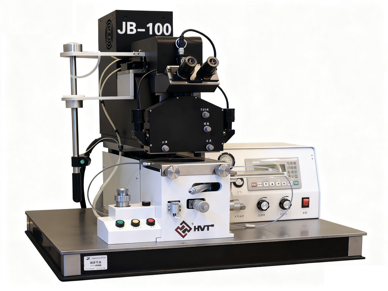
The JB-100 Photolithography Machine is a core exposure equipment for university microelectronics wafer fabrication training lines — it realizes pattern exposure on photoresist-coated wafers via contact alignment, with high-precision positioning and stable light output to match academic teaching & 1μm process lab prototyping.
Specification Item | Details |
Model Number | JB-100 |
Application | Pattern exposure for photoresist-coated wafers (university microelectronics wafer fabrication line) |
Applicable Wafer Size | MAX 4" (100mm) / MAX 5" (125mm×125mm) |
Worktable Stroke | X: ±5mm; Y: ±5mm; Z: 3mm; θ: ±12° |
Wafer & Mask Alignment Gap | 0~0.05mm |
Alignment Precision | ±1μm (for 4" wafers, thickness ≤1μm) |
Exposure Light Source | UVLED (intensity: 40mW/cm²) |
Exposure Uniformity | ≤3% |
Exposure Time | 0-999s (adjustable) |
Power Input | AC220V / 1000W |
Machine Dimensions (L×W×H) | 740mm × 630mm × 1300mm |
Machine Weight | 350KG |
Matching 1μm Wafer Process Training Supports ≤1μm thickness wafers & 1μm alignment precision, perfectly fits the teaching demand of university microelectronics 1μm process fabrication lines
High-Precision Alignment & Exposure Binocular microscope + multi-axis worktable adjustment ensures accurate pattern transfer; stable UVLED light source guarantees consistent exposure effects
User-Friendly for Teaching Visual alignment (via microscope) + adjustable parameters (time/uniformity) lower the operation threshold for students, suitable for classroom demonstrations and lab experiments
Package: 1 set of JB-100 Photolithography Machine (including worktable, light source, and alignment system)
Service: On-site installation (for production line integration) + operation training (for teachers/students) + 1-year warranty