0086-731-52373830 info@sunyinstrument.com

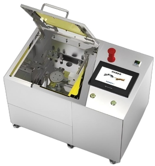
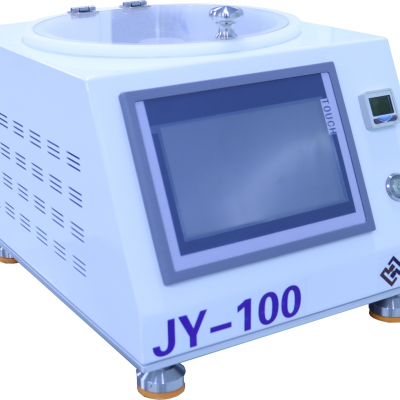
The JX-100 Photoresist Developer is a dedicated developing equipment for university IC (integrated circuit) fabrication teaching lines — it completes the developing process of exposed wafers, with precise parameter control and safety protection, perfectly fitting academic teaching and lab training scenarios.
Specification Item | Details |
Model Number | JX-100 |
Application | Developing operation for exposed wafers (university IC fabrication teaching line) |
Applicable Wafer Size | 85-100mm |
Spindle Rotation Speed | 3000±1rpm |
Wafer Chucking Method | Vacuum adsorption |
Wafer Status Detection Method | Digital vacuum pressure sensor |
Chamber Material | PP (corrosion-resistant) |
Nozzle Quantity | 2 columns (1 developer nozzle + 1 pure water nozzle) |
Safety Configuration | Equipped with dedicated fume hood (to protect operator health) |
Power Input | AC220V, 2KW |
Machine Dimensions (L×W×H) | 600mm × 400mm × 400mm |
Machine Weight | 70KG |
Tailored for IC Teaching Processes Matches the 1μm process IC teaching wafer line, supports standard lab wafer sizes, and fits the developing step in IC fabrication courses
Stable & Controlled Developing Vacuum adsorption ensures wafer stability during high-speed rotation; dual nozzles (developer/pure water) enable seamless process switching
Lab Safety-Focused Design PP corrosion-resistant chamber + dedicated fume hood solve the safety risk of developer volatiles, suitable for student teaching environments
Package: 1 set of JX-100 Photoresist Developer (including developing system, vacuum adsorption module, and fume hood)
Service: On-site installation (for teaching line integration) + operation training (for teachers/students) + 1-year warranty